Double Sided PCB: Structure, Uses, and Why It Remains a Core Technology in Modern Electronics
A Double Sided PCB is one of the most widely used circuit board types in the electronics industry, acting as a powerful balance between simple single-layer PCBs and more advanced multilayer boards. With conductive copper traces on both the top and bottom surfaces, a double-sided PCB provides greater design flexibility, improved routing space, and enhanced circuit performance. From consumer gadgets to industrial machinery, this board type supports thousands of applications where reliable signal flow and moderate circuit density are essential.
What Is a Double Sided PCB?
A Double-Sided PCB is a printed circuit board that features copper traces and components on both sides of the substrate. Unlike single-layer PCBs, which only allow routing on one surface, double-sided boards let designers place vias and interconnections that link both sides, making the board far more versatile. This dual-layer construction supports more complex designs without the cost or complexity of multilayer PCBs. The result is a reliable and cost-effective solution for projects requiring medium circuit density.
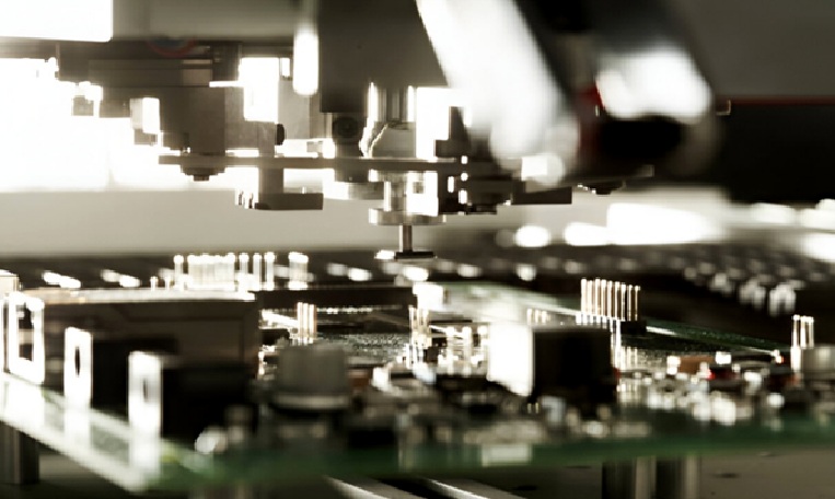
How a Double Sided PCB Is Made
Core Material and Copper Lamination
The Double Sided PCB manufacturing process begins with a base material such as FR-4, polyimide, or other specialized substrates, laminated with copper on both sides. This creates two independent conductive layers that can later be patterned into the desired circuitry. High-quality materials ensure stability, heat resistance, and electrical integrity during device operation.
Imaging and Etching the Circuit Pattern
Once the copper is laminated, an imaging process is used to define the circuitry on each side. Photolithography or laser direct imaging transfers the PCB design onto a photosensitive layer. Afterwards, chemical etching removes the unwanted copper, leaving only the required traces intact. This step must be carefully controlled to avoid over-etching or misalignment, which can affect the performance of the final board.
Drilling and Through-Hole Plating
Drilling plays a critical role in double-layer PCB fabrication. Holes are drilled through the board to allow electrical connection between the top and bottom layers. These through-holes are then plated with copper to create conductive vias. Proper plating thickness ensures low resistance and long-term dependability, especially in high-current or high-vibration applications.
Solder Mask and Surface Finish
A solder mask is applied to both sides of the Double Sided PCB to prevent solder bridging and protect the copper circuitry. After this, a surface finish such as HASL, ENIG, OSP, or immersion silver is added to the exposed copper pads, preparing the board for component soldering. This finish improves solderability, prevents oxidation, and enhances the shelf life of the PCB.
Why Double Sided PCBs Are Still So Important
A Double Sided PCB offers significant advantages for today’s electronic designs. By allowing routing on two surfaces instead of one, it increases available wiring space and supports more compact layouts. This reduces the overall size of the product, lowers manufacturing costs, and improves signal performance. Double-sided boards are ideal for applications where medium complexity and moderate density are required, providing the right balance of performance and affordability.
These PCBs also improve thermal behavior compared to single-layer boards, especially when designed with strategic via placement. They allow designers to separate analog and digital grounds, minimize interference, and optimize current flow. Thanks to this flexibility, double-layer boards remain a go-to solution for engineers across industries.
Applications of Double Sided PCBs
The versatility of Double Sided PCB technology makes it suitable for a wide range of applications. Consumer electronics such as home appliances, televisions, smart lighting, and Bluetooth devices frequently use double-layer boards due to their cost-effectiveness. Industrial automation systems rely on them for motor drivers, control modules, and power supplies because of their durability and electrical stability.
Automotive electronics, communication equipment, medical devices, and security systems also incorporate double-sided PCBs for reliable performance under varying conditions. The ability to support complex routing without the cost of multilayer boards makes them ideal for both prototype development and mass production.
Choosing the Right Double Sided PCB for Your Project
Selecting the right Double Sided PCB involves evaluating several factors, including copper thickness, via structure, operating temperature, and surface finish. High-current circuits may require thicker copper, while sensitive electronics benefit from controlled impedance and precise trace geometry. The choice of substrate will depend on the application environment—standard FR-4 is effective for most conditions, while high-temperature materials are better for demanding industrial or automotive equipment.
Collaborating with an experienced manufacturer ensures proper material selection, precise drilling, reliable plating, and consistent electrical performance. The quality of the bare board directly influences assembly results, product life cycle, and long-term dependability.
Conclusion: Build Your Next Project on a Trusted Double Sided PCB
A Double Sided PCB remains an essential part of modern electronic engineering, offering the perfect combination of performance, flexibility, and affordability. Whether you are developing a new prototype or preparing for large-scale production, choosing a board with high-quality fabrication and precise engineering ensures long-lasting reliability. For the best support, material options, and fabrication expertise, partnering with a trusted Double Sided PCB manufacturer will help ensure your project meets the highest standards of performance and efficiency.