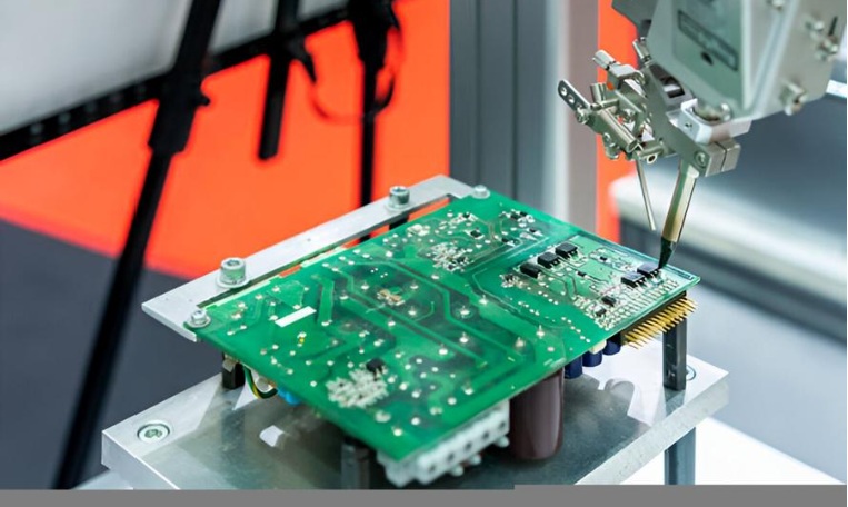
Embedded PCB: Technology, Structure, and Benefits for Modern Electronics
An Embedded PCB is an advanced printed circuit board in which electronic components such as resistors, capacitors, ICs, or semiconductor dies are integrated directly into the inner layers of the board instead of being mounted on the surface. This design approach allows engineers to achieve higher performance, improved reliability, and significant space savings. As devices become smaller yet more powerful, the demand for Embedded PCB technology continues to rise across industries like communications, automotive, medical electronics, aerospace, and IoT.
Why Embedded PCB Technology Is Transforming Electronics
The increasing complexity of modern electronics requires solutions that go beyond traditional surface-mounted design. An Embedded PCB brings the advantage of placing components inside the board structure, resulting in shorter electrical paths, better heat dissipation, and reduced parasitic effects. Because embedded components are shielded within the PCB layers, the system benefits from improved signal integrity and long-term reliability. This capability makes Embedded PCBs particularly attractive for high-frequency, high-density, and mission-critical applications. Engineers rely on this technology to reduce device footprint while achieving exceptional electrical performance.
How Embedded PCB Technology Works
Embedding Passive and Active Components
The foundation of an Embedded PCB lies in its ability to incorporate passive components like resistors and capacitors directly into the dielectric layers. These components are often formed using thin-film or thick-film processes. For active components such as IC chips or semiconductor dies, cavities are milled into the multilayer core, allowing these components to sit securely before the PCB undergoes lamination. This creates a fully integrated structure, where components remain protected from external mechanical and environmental stress.
Sequential Lamination for Structural Integrity
To build an Embedded PCB, manufacturers use multiple lamination cycles to create the required layer stack. Once embedded components are placed, the board undergoes lamination under heat and pressure, ensuring that internal components are securely locked within the PCB. Additional build-up layers are added to route signals to and from the embedded components. This process allows high-density circuit design without increasing the surface component count.
Microvia Technology and Fine Routing
Microvias play a critical role in Embedded PCB construction. These tiny, laser-drilled vias connect inner embedded components to outer circuit layers with extreme precision. Microvias enable designers to achieve ultra-short electrical connections, improving signal transmission and minimizing losses. With microvia structures and fine trace widths, Embedded PCBs can support dense routing for high-speed, high-performance systems.
Thermal and Electrical Considerations
When active devices are embedded, heat becomes a key concern. Embedded PCBs use specialized thermal vias, thermally conductive dielectrics, and copper coins to transfer heat away from internal components. Electrically, embedded positioning minimizes stray inductance and capacitance, improving overall system stability. This makes Embedded PCBs ideal for applications requiring clean power, stable signals, and controlled impedance.
Advantages of Using Embedded PCB Technology
Superior Electrical Performance
By embedding components within the PCB layers, engineers can greatly reduce signal paths and parasitic effects. This improves power integrity and allows for high-speed performance in communication systems, processors, and sensor modules. The consistency and reliability of electrical behavior remain stable even under demanding operating conditions.
Effective Heat Management
Because embedded structures allow heat to move more efficiently across the PCB, the overall thermal profile becomes more controlled. This is essential for high-power electronics and compact devices that cannot depend solely on surface cooling methods.
Miniaturization and Higher Functional Density
One of the biggest advantages of an Embedded PCB is its ability to increase circuit density without adding more surface components. This supports the design of smaller, lighter, and more compact devices. Embedded PCB technology is widely used in wearables, medical implants, automotive ECUs, and aerospace control systems where space and weight are critical.
Improved Reliability and Protection
Once components are embedded, they become shielded from external vibration, mechanical shock, moisture, contamination, and corrosion. This internal placement increases durability and long-term performance, making Embedded PCBs suitable for harsh environments and mission-critical fields like defense, avionics, and industrial automation.
Applications of Embedded PCB Technology
Consumer Electronics and IoT Devices
Smartphones, wearables, and ultra-compact IoT sensors use Embedded PCBs to fit more functions into smaller spaces. This supports sleek designs without compromising performance.
Automotive and EV Electronics
Electric vehicles, ADAS systems, radar modules, and powertrain controllers use Embedded PCBs to improve heat management and ensure reliable performance in challenging operating conditions.
Medical and Healthcare Electronics
Medical implants, diagnostic devices, and portable monitoring systems rely on embedded solutions for precision, stability, and miniaturization. Internalized components help maintain accuracy and reduce the risk of mechanical failure.
Aerospace and Defense Systems
In aerospace environments where vibration, temperature changes, and reliability are critical, Embedded PCBs provide structural stability and secure component integration.
Design Challenges and Key Considerations
Material Selection and Thermal Behavior
Choosing the right dielectric materials is vital for balancing thermal performance and electrical behavior. High-temperature laminates, low-loss materials, and stable dielectrics help ensure compatibility with embedded components.
Layout Precision and Manufacturing Accuracy
Designers must account for cavity sizes, microvia positions, and layer alignment to ensure embedded components integrate perfectly. Any misalignment can affect routing or device stability.
Testing and Quality Assurance
Because embedded components are not visible, advanced testing methods like 3D X-ray inspection, AOI, and electrical testing ensure the board is defect-free before final assembly.
Conclusion: Build High-Performance Devices with Advanced Embedded PCB Technology
Embedded PCB technology is reshaping the future of electronics by offering unmatched performance, reliability, and space efficiency. As industries push toward faster, smaller, and more durable systems, Embedded PCBs provide the ideal foundation for innovation. If your next project requires precision engineering, enhanced signal integrity, and compact system design, partnering with a skilled Embedded PCB Manufacturer will ensure you receive the high-quality, high-reliability solutions your application demands.


![[pii_email_00f325435e1254f27c95] Error](https://trendy2news.com/wp-content/uploads/2021/10/Right-Solutions-of-the-pii_email_00f325435e1254f27c95-Error-768x371.jpg)

